|
Product Description:
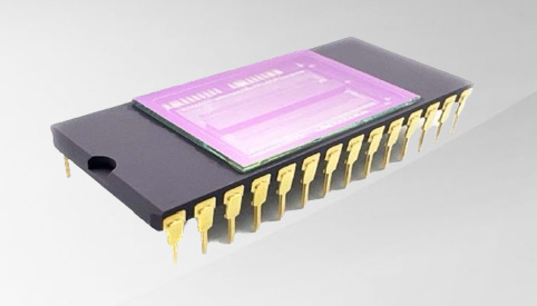
Precision Micro-Optics offers uncooled near-infrared linear image sensor consisting of a linear InGaAs-detector array bonded to the p-on-n readout IC.
Product Features:
- 1024X1 Pixels (12.5X12.5um or 12.5X250um)
- 28-pin Ceramic DIP (CDIP)
- Built-in Temperature Sensor
- 0.9 μm – 1.7 μm Spectral Range
- Minimum Pixel Operability > 99%
- Quantum Efficiency > 70%
- Snapshot ITR / IWR
- 2 Outputs with up to 22 MHz Pixel Rate
Applications:
- Shortwave-Infrared Imaging
- Near-Infrared Spectrophotometry
- Semiconductor Inspection / Process Monitoring
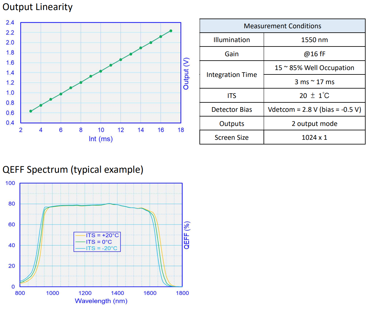
SPECIFICATIONS (ITS = 20 ± 1ºC)(Readings from Integrated Temperature Sensor (ITS)):
Parameters
|
Symbol
|
Test conditions
|
Min
|
Typ |
Max
|
Unit |
Sensor Technology
|
|
|
Planar InGaAs PIN
|
|
Actual Pixel Array
|
|
|
1024 x 1
|
|
Pixel Pitch
|
|
|
12.5
|
um
|
Pixel Size (S)
|
|
|
12.5 X12.5
|
um
|
Pixel Size (M)
|
|
|
12.5 X250
|
um
|
Spectral Response Range
|
λ
|
|
900
|
|
1700
|
nm
|
Dark Current (S)(*)
|
ID
|
VR = 0.5V
|
|
|
0.6
|
nA
|
Dark Current (M)(*)
|
ID
|
VR = 0.5V
|
|
|
1
|
nA
|
Quantum Efficiency * Fill Factor(*)
|
QEFF
|
λ = 1550nm
|
70 |
|
|
%
|
Response Nonuniformity(*)
|
|
At 50 % Full Well
|
|
|
5
|
%
|
Response Nonlinearity
|
|
15 % – 85 % Well Occupation Range
|
|
|
2
|
%
|
Charge Capacity
(16 settings)
|
|
Cint = 6.4 fF
|
|
25
|
|
μV/e-
|
Cint = 16 fF
|
|
10
|
|
Cint = 30 fF
|
|
5.3
|
|
Cint = 120 fF
|
|
1.3
|
|
Cint = 2.1 pF
|
|
0.076
|
|
Readout Noise
(ROIC Specifications )
|
|
Cint = 6.4 fF
|
|
1.2
|
|
mV
|
Cint = 16 fF
|
|
0.8
|
|
Cint = 30 fF
|
|
0.6
|
|
Cint = 120 fF
|
|
0.5
|
|
Cint = 2.1 pF
|
|
0.25
|
|
Output Swing
|
|
Gain @16 fF (High Gain Mode)
|
2.0
|
|
|
V
|
Minimum Integration Period
|
|
ROIC Specifications |
5 |
|
|
μs
|
Maximum Pixel Rate
|
|
ROIC Specifications |
|
|
22
|
MHz
|
Pixel Operability(*)
|
VBD
|
Percentage of Pixels with QEFF
Deviation ± 20%*(QEFF Mean) |
99
|
|
|
%
|
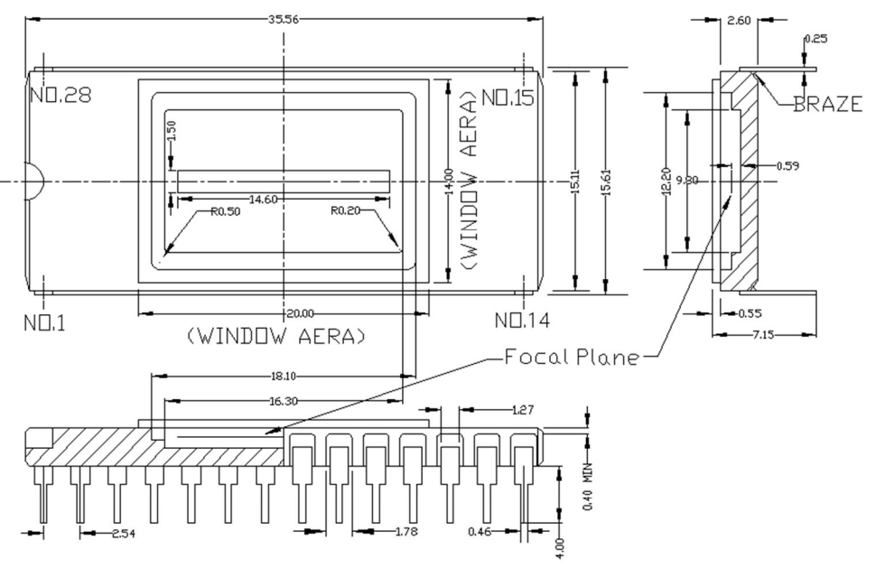
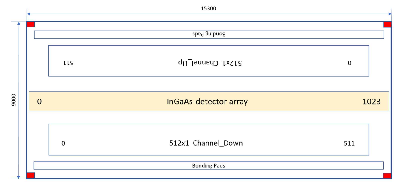
Chip Size
|
|
|
15.3 x 9.0
|
mm
|
Package Type
|
|
|
28-pin Ceramic DIP (CDIP)
|
|
Package Size L x W x T
|
|
|
35.56 x 15.61 x 7.15
|
mm
|
Weight
|
|
|
5.18
|
g
|
Note (*): These items are defined for central effective pixel array (1024x1). Their values correspond to default operation conditions.
Absolute Maximum Ratings (T=25ºC):
| |
Parameters
|
Min
|
Typ |
Max
|
Unit |
| |
Operating Temperature
|
-40
|
|
70
|
°C
|
| |
Storage Temperature
|
-40
|
|
70
|
°C
|
| |
Power Consumption
|
|
|
190
|
mW
|
Package Dimensions (mm) and Pin Definition:
| |
01
|
VDD_D
|
08
|
SDOUT_D |
15
|
GND
|
22
|
SDIN_U |
| |
02
|
RESET_D
|
09
|
DATVALID_D |
16
|
VR1_U
|
23
|
CEB_U |
| |
03
|
NC
|
10
|
VOUT_D |
17
|
VR2_U
|
24
|
MC_U |
| |
04
|
INT_D
|
11
|
VDDA_D |
18
|
VTEMP_U
|
25
|
INT_U |
| |
05
|
MC_D
|
12
|
VR2_D |
19
|
VDDA_U
|
26
|
NC |
| |
06
|
CEB_D
|
13
|
VR1_D |
20
|
VOUT_U
|
27
|
RESET_U |
| |
07
|
SDIN_D
|
14
|
VDETCOM |
21
|
SDOUT_U
|
28
|
VDD_U |
CHIP LAYOUT:
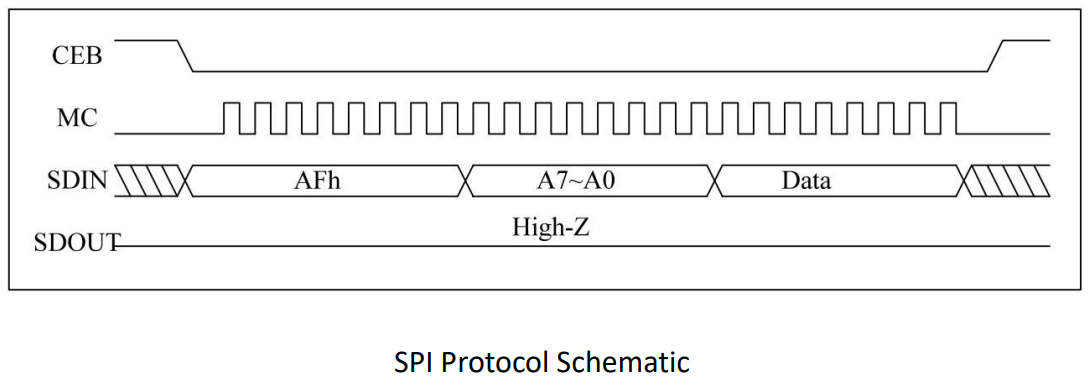
SPI Interface:
The Linear Image Sensor supports SPI protocol to set the command registers. There are functions of the gain mode,
power consumption control and the sequence of pixel output. The 1024x1 photodiode array is
connected to two 512x1 readout ICs.
Bias Input :
| |
Pin #
|
Bias
|
Voltage |
Current
|
Remark |
| |
01, 28
|
VDD_D, VDD_U
|
1.8 V |
> 30 mA
|
Positive logic supply
|
| |
11, 19
|
VDDA_D, VDDA_U
|
3.6 V |
> 60 mA
|
Positive analog supply
|
| |
12, 17
|
VR2_D, VR2_U
|
0.3 V |
> 30 mA
|
External Input Bias
|
| |
13, 16
|
VR1_D, VR1_U
|
2.3 V |
> 5 mA
|
External Input Bias
|
| |
14
|
VDETCOM
|
> VR1_D&U |
|
Detector common voltage
Detector bias = VDETCOM - VR1_D&U (*)
|
| |
15
|
GND
|
0V |
|
Ground
|
| |
02, 27
|
RESET_D, RESET_U
|
1.8 V |
|
Chip reset
|
Note (*): VDETCOM lower than 2.3 V will forward bias the sensor, the exact zero bias voltage is device and temperature dependent.
Digital Pattern Input :
| |
Pin #
|
Clocks
|
Levels |
Rise/Fall
|
Remark |
| |
04, 25
|
INT_D, INT_U
|
1.8 V / 0 V |
< 50 nS
|
Integration time
|
| |
05, 24
|
MC_D, MC_U
|
1.8 V / 0 V |
< 5 nS
|
Master clock,
Max. Freq. = 22 MHz
|
| |
06, 23
|
CEB_D, CEB_U
|
1.8 V / 0 V |
< 10 nS
|
Chip enable(*)
|
| |
07, 22
|
SDIN_D, SDIN_U
|
1.8 V / 0 V |
< 5 nS
|
Data code input
|
Note (*): The input and output of all commands start after the falling edge of CEB.
Digital Pattern Output :
| |
Pin #
|
Clocks
|
Levels |
Rise/Fall
|
Remark |
| |
08, 21
|
SDOUT_D, SDOUT_U
|
1.8 V / 0 V |
|
Data code output
|
| |
09
|
DATVALID_D
|
1.8 V / 0 V |
|
Valid data output flag signal
|
Analog Output :
| |
Pin #
|
Outputs
|
Levels |
Value
|
Remark |
| |
10, 20
|
VOUT_D, VOUT_U
|
0.2 ~ 2.4 V |
|
Video output
|
| |
18
|
VTEMP_U
|
2.138 V |
27℃
|
Integrated Temperature Sensor (-0.6 mV /℃)
|
Figures :
|